By Amit Nath
For investors who have followed Montaka for some time, they will be aware that our investment philosophy is based on investing in advantaged companies with strong competitive positions in industries undergoing structural transformation.
As we speak, the semiconductor industry is undergoing one of its most profound structural transformations in decades.
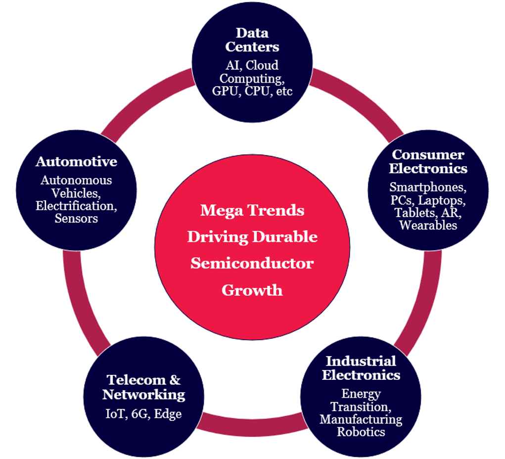
Semiconductors are the bedrock of our digital world. They are the silent enablers of many global megatrends – from cloud computing, to autonomous vehicles and the ongoing energy transition.
But it is the surge towards an AI-native future that is creating massive demand for chips and is also accelerating a fundamental shift in how chips are designed, manufactured, and assembled.
“AI is the most transformative technology of the last 50 years, and we are in the very early stages of the largest deployment of compute capacity in history[1],” says Lisa Su, the CEO of semiconductor company AMD.
The total semiconductor market is forecast to reach US$1 trillion by 2030, a compound annual growth rate (5-year CAGR) of 9%[2].
The transformation has already created huge winners, including helping Nvidia to become the world’s largest company by market cap.
But we believe the AI-driven structural transformation of the semiconductor industry will continue to throw up other amazing long-term investment opportunities for investors, and is therefore vital to understand.
Data Centers create chip demand surge
For years, consumer devices such as smartphones and PCs dictated the semiconductor industry’s rhythm.
Today, however, the industry’s pulse has quickened.
The massive, ongoing explosion in data center construction is directly driving an unprecedented demand for semiconductor chips.
These facilities, which form the physical backbone of cloud computing, streaming services, and artificial intelligence (AI), require chips to power every aspect of their operation.
At the heart of each data center are thousands of servers, all packed with high-performance processors, primarily Central Processing Units (CPUs) for general tasks, and specialized Graphics Processing Units (GPUs) for the parallel processing needed by intensive AI and machine learning workloads.
Because AI’s resource requirements are exponentially higher than traditional cloud services, the need for these powerful AI accelerators (GPUs) has become the single biggest factor in rising chip demand and semiconductor fabrication today.
The automotive sector is another growth engine for semiconductors as cars become computers on wheels, filled with chips for autonomous driving and a projected CAGR of 9%[3].
The core semiconductor markets of smartphones and personal computers are maturing with CAGRs of 5% and 4% respectively. This translates into a non-data center semiconductor CAGR of only 6%[4].
But demand for AI processing and data centers is exploding, driving this end-market to a projected 18% CAGR through 2030[5], which implies an increase of 2.3x in total size.
Some even believe that these estimates may prove to be massively underbaked.
Intel recently noted “projections are calling for a greater than 10x increase of gigawatts of AI [data center] capacity by 2030[6]”.
In other words, the market might be 4-5x larger than many are currently thinking.
Torrent of capital
AI is the ultimate ‘horizontal innovation’, a technological wave that lifts all boats by permeating every market and demanding ever-increasing semiconductor content in all electronic equipment.
To meet this demand, the industry is unleashing a torrent of capital.
As noted, global spending on semiconductors is projected to exceed a staggering $1 trillion by 2030 (5 yr CAGR of 9%), and while this number is shockingly large, the estimates came before OpenAI revealed its plans to incrementally add over $1.4 trillion of data center capacity[7] on its own over the coming 5-10 years (which includes land, building, energy, and cooling in addition to chips).
It’s possible that OpenAI may represent an incremental $350 to 400 billion of data center semiconductor demand not factored into industry estimates.
Including this, the total market for semiconductors may increase to $1.2 trillion (5 yr CAGR of 12%) with data center semiconductor CAGR accelerating from 18% to 27% over the period, representing a 3.3x increase in size.
This is still well below the 10x increase in data center capacity Intel indicated was on the table by 2030.
Semiconductor Market Accelerated by OpenAI Data Center Plans
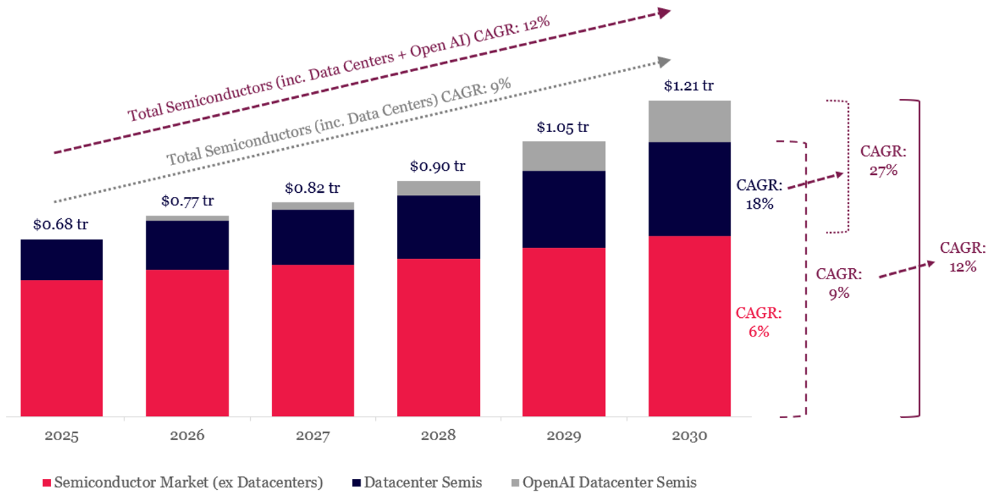
Source: ASML, Montaka Global
The limits of Moore’s Law
AI is not just creating huge demand for chips; it is also accelerating another profound shift in the architecture of chips.
For decades, the semiconductor industry’s mantra was Moore’s Law: that the number of transistors (microscopic electronic switches) on a silicon chip doubles every two years.
This gave the industry a formula: shrink the transistors, double the density, rinse-and-repeat.
This process of ‘node scaling’ drove incredible performance gains and enabled a myriad of electronic applications such as laptops, smartphones and tablets.
Node scaling from 90-nanometer (nm) chips to 28nm often doubled transistor density while improving performance by 25-50%.
But Moore’s law has reached its limits.
As the industry pushed below 14nm, this paradigm began to show diminishing marginal returns.
The cost of manufacturing a wafer has nearly quadrupled from the 14nm node to today’s 3nm node, while performance improvements have approached zero.
Moore’s Law and Diminishing Marginal Returns
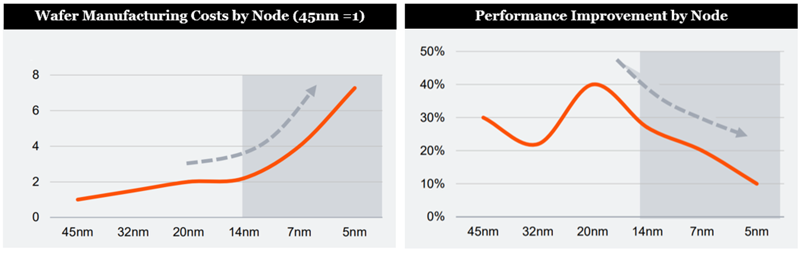
Source: AMD, PWC
Today, a single 3nm transistor wafer costs over US$24,000, a stark contrast to the previously cutting-edge 16nm version, which cost US$6,000 when it was released a decade ago.
A major strategic pivot
With Moore’s Law coming to an end, the industry has been forced into a strategic pivot.
It has shifted from pure-play transistor scaling to a more holistic, system-level approach.
‘Advanced packaging’ has emerged as a prime lever for performance.
Basically, if you can no longer cram more transistors onto a single chip, the solution is to stack multiple specialized “chiplets” together in a single package and have them talk to each other without having to leave the packaging via optical fiber or copper cable (which adds time overhead and dramatically reduces performance, also known as latency).
Packaging technologies – exemplified by TSMC’s Chip-on-Wafer-on-Substrate (CoWoS) and future System-on-Wafer (SoW-X) – are now central to chip construction roadmaps.
Future generations are expected to deliver performance scaling from 1x to over 40x, significantly better than Moore’s Law.
Advanced Packaging Innovation Enabling Massive Scaling
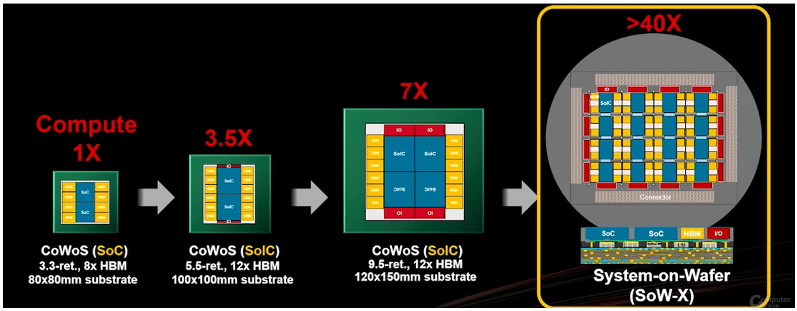
Source: TSMC
The limitations of Moore’s Law made an architectural shift inevitable for the field to advance.
But the exploding demand for AI caused the industry and chip designers to push innovation to new limits at a hyper-accelerated rate.
There is no better example of beating Moore’s Law than Nvidia.
It has added trillions of dollars of market value and become the world’s largest company in a very short time as AI demand surged.
As Nvidia CEO Jensen Huang noted: “Our systems are progressing way faster than Moore’s Law. We can build the architecture, the chip, the system … then you can move faster than Moore’s Law, because you can innovate across the entire [AI] stack[8]”
Structural transformation will continue to open up fruitful opportunities
The semiconductor industry is undergoing a structural transformation, driven by AI’s unprecedented demand for compute.
This era moves beyond Moore’s Law, focusing on advanced packaging and system-level innovation to build the foundational architecture for an AI-native future.
The rise of AI has created a new gold rush in the semiconductor sector, shifting investment opportunities far beyond just GPU producers like Nvidia.
An AI-driven world presents opportunities across the entire semiconductor value chain, from specialized hardware and manufacturing tools to the foundational infrastructure supporting massive data center growth.
At Montaka, we believe this large, structural transformation will persist for many, many years and represents a particularly fruitful opportunity space to unearth investment candidates, which we are actively exploring.
Note:
[1] Lisa Su, CEO of AMD, conference call discussing strategic partnership between AMD and OpenAI, October 6, 2025
[2] ASML Investor Day, November 14, 2024
[3] ASML Investor Day, November 14, 2024
[4] ASML Investor Day, November 14, 2024
[5] ASML Investor Day, November 14, 2024
[6] David Zinser, CFO of Intel Corp., conference call discussing Q3 2025 earnings results, October 23, 2025
[7] Sam Altman, CEO of OpenAI, October 23, 2025
[8] Jenson Huang, CEO of Nvidia, January 6, 2025
Amit Nath is the Director of Research at Montaka Global Investments. To learn more about Montaka, please call +612 7202 0100.
Podcast: Join the Montaka Global Investments team on Spotify as they chat about the market dynamics that shape their investing decisions in Spotlight Series Podcast. Follow along as we share real-time examples and investing tips that govern our stock picks. Click below to listen. Alternatively, click on this link: https://podcasters.spotify.com/pod/show/montaka
To request a copy of our latest paper which explores the empirical research around the 3 pillars of active management outperformance, please share your details with us:

From Transistors to Transformations: Building AI’s Digital Backbone
By Amit Nath
For investors who have followed Montaka for some time, they will be aware that our investment philosophy is based on investing in advantaged companies with strong competitive positions in industries undergoing structural transformation.
As we speak, the semiconductor industry is undergoing one of its most profound structural transformations in decades.
Semiconductors are the bedrock of our digital world. They are the silent enablers of many global megatrends – from cloud computing, to autonomous vehicles and the ongoing energy transition.
But it is the surge towards an AI-native future that is creating massive demand for chips and is also accelerating a fundamental shift in how chips are designed, manufactured, and assembled.
“AI is the most transformative technology of the last 50 years, and we are in the very early stages of the largest deployment of compute capacity in history[1],” says Lisa Su, the CEO of semiconductor company AMD.
The total semiconductor market is forecast to reach US$1 trillion by 2030, a compound annual growth rate (5-year CAGR) of 9%[2].
The transformation has already created huge winners, including helping Nvidia to become the world’s largest company by market cap.
But we believe the AI-driven structural transformation of the semiconductor industry will continue to throw up other amazing long-term investment opportunities for investors, and is therefore vital to understand.
Data Centers create chip demand surge
For years, consumer devices such as smartphones and PCs dictated the semiconductor industry’s rhythm.
Today, however, the industry’s pulse has quickened.
The massive, ongoing explosion in data center construction is directly driving an unprecedented demand for semiconductor chips.
These facilities, which form the physical backbone of cloud computing, streaming services, and artificial intelligence (AI), require chips to power every aspect of their operation.
At the heart of each data center are thousands of servers, all packed with high-performance processors, primarily Central Processing Units (CPUs) for general tasks, and specialized Graphics Processing Units (GPUs) for the parallel processing needed by intensive AI and machine learning workloads.
Because AI’s resource requirements are exponentially higher than traditional cloud services, the need for these powerful AI accelerators (GPUs) has become the single biggest factor in rising chip demand and semiconductor fabrication today.
The automotive sector is another growth engine for semiconductors as cars become computers on wheels, filled with chips for autonomous driving and a projected CAGR of 9%[3].
The core semiconductor markets of smartphones and personal computers are maturing with CAGRs of 5% and 4% respectively. This translates into a non-data center semiconductor CAGR of only 6%[4].
But demand for AI processing and data centers is exploding, driving this end-market to a projected 18% CAGR through 2030[5], which implies an increase of 2.3x in total size.
Some even believe that these estimates may prove to be massively underbaked.
Intel recently noted “projections are calling for a greater than 10x increase of gigawatts of AI [data center] capacity by 2030[6]”.
In other words, the market might be 4-5x larger than many are currently thinking.
Torrent of capital
AI is the ultimate ‘horizontal innovation’, a technological wave that lifts all boats by permeating every market and demanding ever-increasing semiconductor content in all electronic equipment.
To meet this demand, the industry is unleashing a torrent of capital.
As noted, global spending on semiconductors is projected to exceed a staggering $1 trillion by 2030 (5 yr CAGR of 9%), and while this number is shockingly large, the estimates came before OpenAI revealed its plans to incrementally add over $1.4 trillion of data center capacity[7] on its own over the coming 5-10 years (which includes land, building, energy, and cooling in addition to chips).
It’s possible that OpenAI may represent an incremental $350 to 400 billion of data center semiconductor demand not factored into industry estimates.
Including this, the total market for semiconductors may increase to $1.2 trillion (5 yr CAGR of 12%) with data center semiconductor CAGR accelerating from 18% to 27% over the period, representing a 3.3x increase in size.
This is still well below the 10x increase in data center capacity Intel indicated was on the table by 2030.
Semiconductor Market Accelerated by OpenAI Data Center Plans
Source: ASML, Montaka Global
The limits of Moore’s Law
AI is not just creating huge demand for chips; it is also accelerating another profound shift in the architecture of chips.
For decades, the semiconductor industry’s mantra was Moore’s Law: that the number of transistors (microscopic electronic switches) on a silicon chip doubles every two years.
This gave the industry a formula: shrink the transistors, double the density, rinse-and-repeat.
This process of ‘node scaling’ drove incredible performance gains and enabled a myriad of electronic applications such as laptops, smartphones and tablets.
Node scaling from 90-nanometer (nm) chips to 28nm often doubled transistor density while improving performance by 25-50%.
But Moore’s law has reached its limits.
As the industry pushed below 14nm, this paradigm began to show diminishing marginal returns.
The cost of manufacturing a wafer has nearly quadrupled from the 14nm node to today’s 3nm node, while performance improvements have approached zero.
Moore’s Law and Diminishing Marginal Returns
Source: AMD, PWC
Today, a single 3nm transistor wafer costs over US$24,000, a stark contrast to the previously cutting-edge 16nm version, which cost US$6,000 when it was released a decade ago.
A major strategic pivot
With Moore’s Law coming to an end, the industry has been forced into a strategic pivot.
It has shifted from pure-play transistor scaling to a more holistic, system-level approach.
‘Advanced packaging’ has emerged as a prime lever for performance.
Basically, if you can no longer cram more transistors onto a single chip, the solution is to stack multiple specialized “chiplets” together in a single package and have them talk to each other without having to leave the packaging via optical fiber or copper cable (which adds time overhead and dramatically reduces performance, also known as latency).
Packaging technologies – exemplified by TSMC’s Chip-on-Wafer-on-Substrate (CoWoS) and future System-on-Wafer (SoW-X) – are now central to chip construction roadmaps.
Future generations are expected to deliver performance scaling from 1x to over 40x, significantly better than Moore’s Law.
Advanced Packaging Innovation Enabling Massive Scaling
Source: TSMC
The limitations of Moore’s Law made an architectural shift inevitable for the field to advance.
But the exploding demand for AI caused the industry and chip designers to push innovation to new limits at a hyper-accelerated rate.
There is no better example of beating Moore’s Law than Nvidia.
It has added trillions of dollars of market value and become the world’s largest company in a very short time as AI demand surged.
As Nvidia CEO Jensen Huang noted: “Our systems are progressing way faster than Moore’s Law. We can build the architecture, the chip, the system … then you can move faster than Moore’s Law, because you can innovate across the entire [AI] stack[8]”
Structural transformation will continue to open up fruitful opportunities
The semiconductor industry is undergoing a structural transformation, driven by AI’s unprecedented demand for compute.
This era moves beyond Moore’s Law, focusing on advanced packaging and system-level innovation to build the foundational architecture for an AI-native future.
The rise of AI has created a new gold rush in the semiconductor sector, shifting investment opportunities far beyond just GPU producers like Nvidia.
An AI-driven world presents opportunities across the entire semiconductor value chain, from specialized hardware and manufacturing tools to the foundational infrastructure supporting massive data center growth.
At Montaka, we believe this large, structural transformation will persist for many, many years and represents a particularly fruitful opportunity space to unearth investment candidates, which we are actively exploring.
Note:
[1] Lisa Su, CEO of AMD, conference call discussing strategic partnership between AMD and OpenAI, October 6, 2025
[2] ASML Investor Day, November 14, 2024
[3] ASML Investor Day, November 14, 2024
[4] ASML Investor Day, November 14, 2024
[5] ASML Investor Day, November 14, 2024
[6] David Zinser, CFO of Intel Corp., conference call discussing Q3 2025 earnings results, October 23, 2025
[7] Sam Altman, CEO of OpenAI, October 23, 2025
[8] Jenson Huang, CEO of Nvidia, January 6, 2025
Amit Nath is the Director of Research at Montaka Global Investments. To learn more about Montaka, please call +612 7202 0100.
Podcast: Join the Montaka Global Investments team on Spotify as they chat about the market dynamics that shape their investing decisions in Spotlight Series Podcast. Follow along as we share real-time examples and investing tips that govern our stock picks. Click below to listen. Alternatively, click on this link: https://podcasters.spotify.com/pod/show/montaka
To request a copy of our latest paper which explores the empirical research around the 3 pillars of active management outperformance, please share your details with us:
This content was prepared by Montaka Global Pty Ltd (ACN 604 878 533, AFSL: 516 942). The information provided is general in nature and does not take into account your investment objectives, financial situation or particular needs. You should read the offer document and consider your own investment objectives, financial situation and particular needs before acting upon this information. All investments contain risk and may lose value. Consider seeking advice from a licensed financial advisor. Past performance is not a reliable indicator of future performance.
Related Insight
Share
Get insights delivered to your inbox including articles, podcasts and videos from the global equities world.